with Xilinx Spartan-7
- Dimensions of 2″ x 2″ (50.8 mm x 50.8 mm)
- 83 User In-/Outputs
- 1 differential analog input
- 4 user LEDs
- 4 user Switches
- USB-UART bridge with up to 3 Mbaud
- Powered via USB or external voltage supply from 5 V to 17 V
- 100 MHz onboard clock
- 64 Mbit configuration memory
- Standard Xilinx JTAG header (14 pin)
- Out-of-the-box functionality, no mother- or carrierboard required
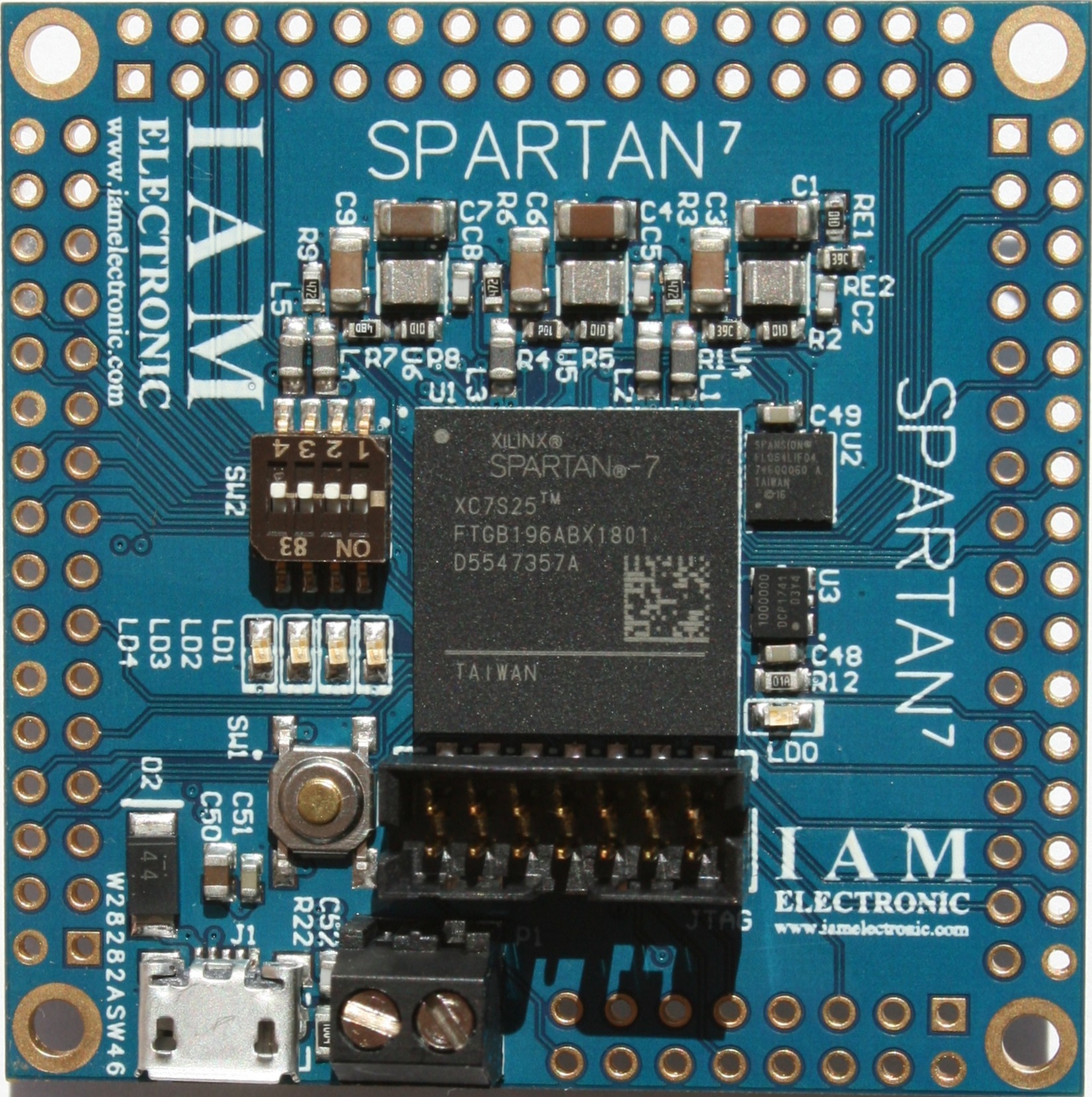
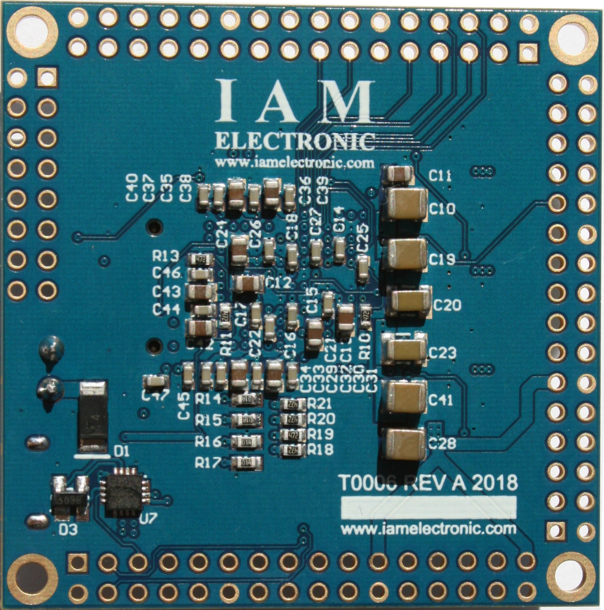
The photos below show both sides of the small form factor Spartan-7 FPGA Module (equipped with Xilinx XC7S25-1FTGB196). By default, the board is not populated with pin headers on the 2.54 mm grid.
- Industrial measurements and control
- Digital signal processing
- Interface adaptation
- Easy prototyping
- Education and research with FPGAs
The small form factor Spartan-7 FPGA Module is an out-of-the-box feature FPGA board with only 2″ x 2″ (50.8 mm x 50.8 mm) dimensions. It is ready for use by simply connecting a power supply and programming the FPGA or the 64 Mbit SPI flash via the standard Xilinx JTAG connector. The board operates with a USB power supply or an external power supply sourced either by the screw terminal P1 or the pin grid. The module supports a wide input voltage range from 5 V up to 17 VDC and provides 83 general purpose IOs (GPIOs) through easily accessible pin grids at the edges of the board. Additionally there is a dedicated input for analog-to-digital conversion with a sample rate of up to 1 MSPS and a resolution of 12 bit (built-in Xilinx XADC module). The onboard USB-UART bridge allows communication to a host with datarates up to 3 MBaud. Further, the Spartan-7 FPGA Module has four programmable blue LEDs and four micro switches for user interactions. The board includes a stable 100 MHz system clock source for the FPGA, but which also can be clocked from external sources via pin connectors. Finally, the board offers all basic functions for many FPGA applications on a tiny footprint without the need for an additional carrier board.
The board can be powered via the USB connector J1 or via an appropriate voltage (5 V to 17 V) at the screw terminal P1. It is not recommended to use both power supply inputs simultaneously! If possible, the USB power supply by a host should be deactivated
when using the screw terminals for powering the board. With sufficient caution, however, both voltage inputs can also be used in parallel. A test with 17 V input voltage and additional USB power supply showed no damage or impairments.
Be careful and make sure that the power supply is connected with the correct polarity! The board has no further input protection circuit for an incorrect connection. The ports of the screw terminal P1 are marked with + and - signs on silkscreen layer (in future version, not yet in rev. A). Fig. 1 shows the right polarity.
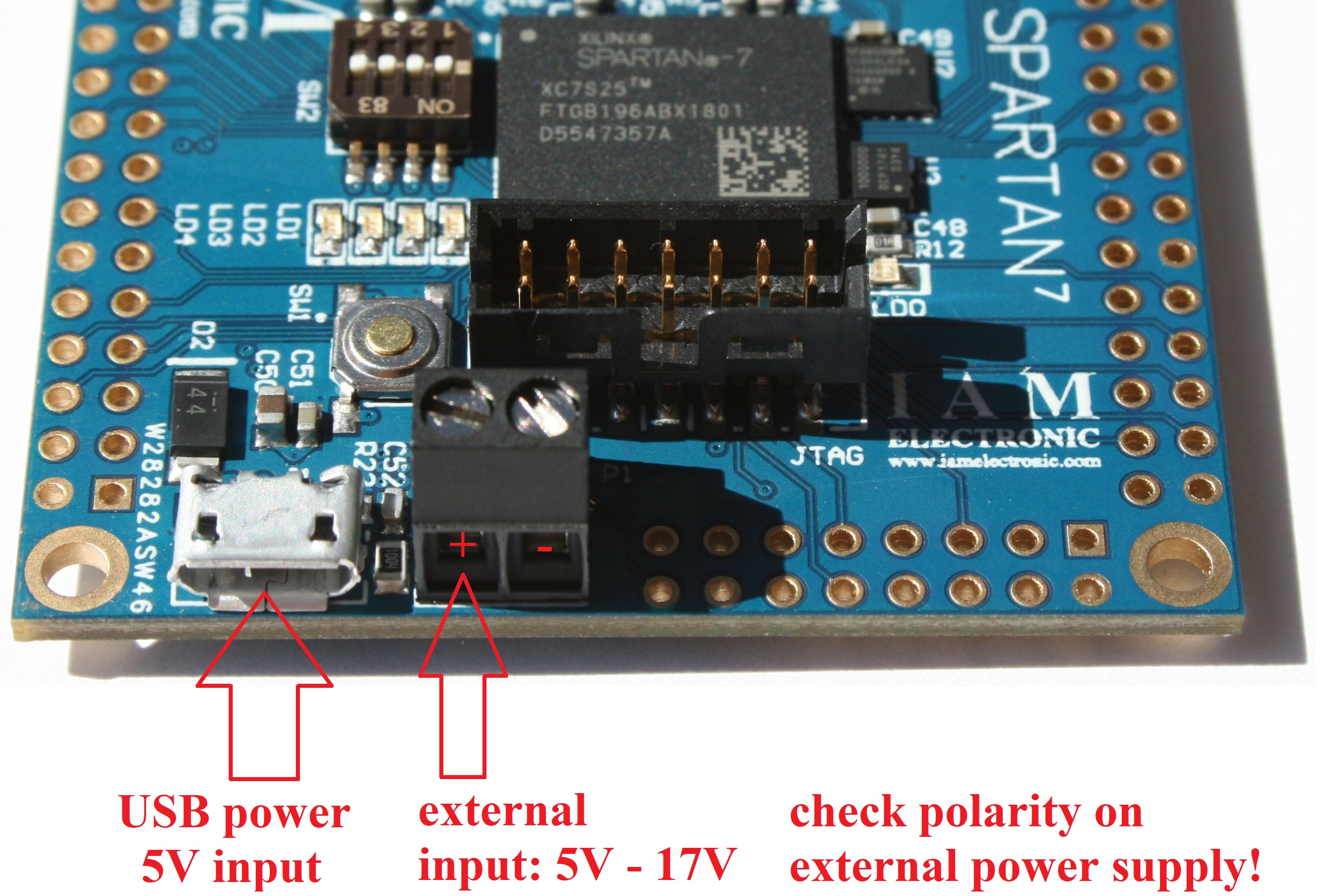 Fig. 1: Take care of the right polarity of the screw terminal power input P1. The positive terminal is located left.
Another way to power the Spartan-7 board is to use the dedicated pins of the pin grid (see Fig. 2). Pin 1 of each grid (square shape) can be used as main voltage input or output. The corresponding Ground (GND) is pin 2. Supply via these pins corresponds functionally
to supply via the screw terminal P1. The valid input voltage range is 5 V to 17 V! The main purpose of these pins is to supply further slave modules or other devices. That means, these pins are intended as voltage output!
It is possible to supply the FPGA module itself via these pins, but this should not be the preferred usage. With a power supply via the USB connector, the output voltage at pin 1 of the pin grid is approx. 5 V. When external voltage
is applied to the screw terminal P1, this voltage will appear on the pins.
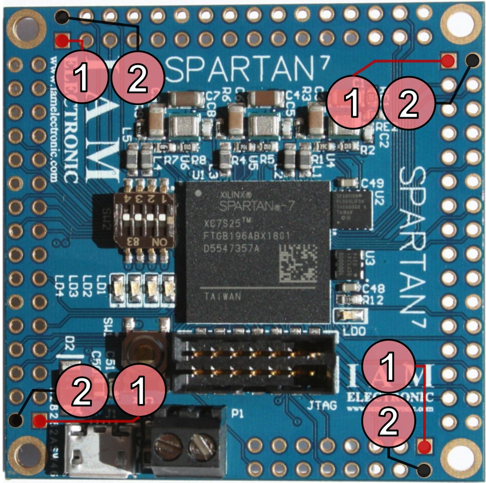 Fig. 2: Pin number markings on the connector grid. Pin 1 of each grid can be used as a power supply output or input. Pin 2 is the corresponding ground (GND).
2.1. Programming the board
Fig. 2: Pin number markings on the connector grid. Pin 1 of each grid can be used as a power supply output or input. Pin 2 is the corresponding ground (GND).
2.1. Programming the board
Our Spartan-7 FPGA Module is supported by the free Xilinx Vivado HL WebPack Edition since Version 2018.1. Code can be synthesized and finally downloaded to the FPGA with the Xilinx toolchain. For this purpose, we recommend
a supported programming cable like Xilinx Platform Cable USB or JTAG-HS3 Programming Cable from Digilent. Your cable must fit into the standard Xilinx JTAG header with 14 pins. Some examples are shown in Fig. 3 below.
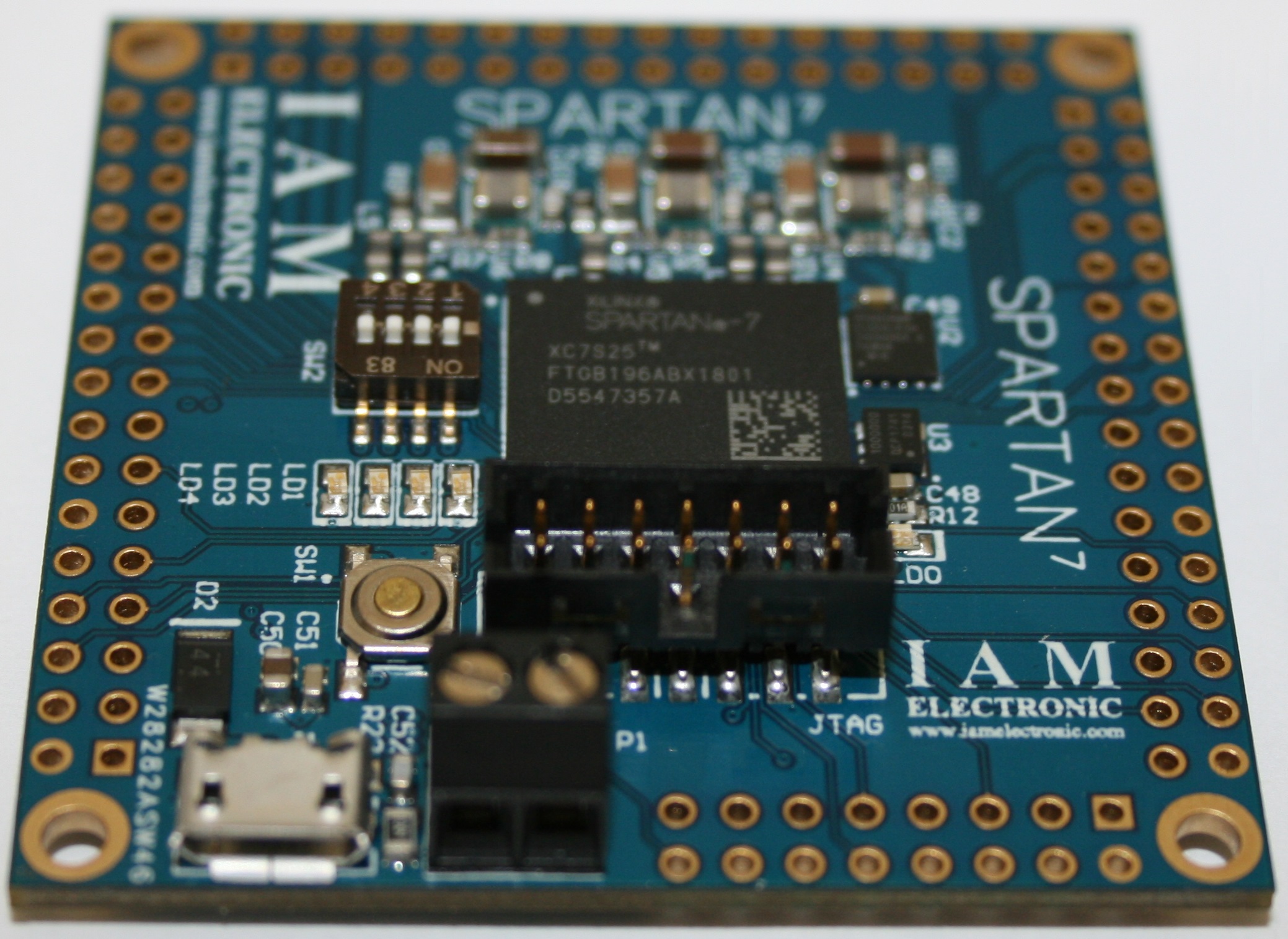
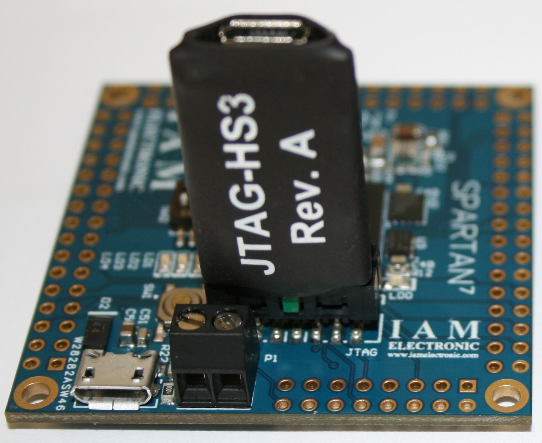
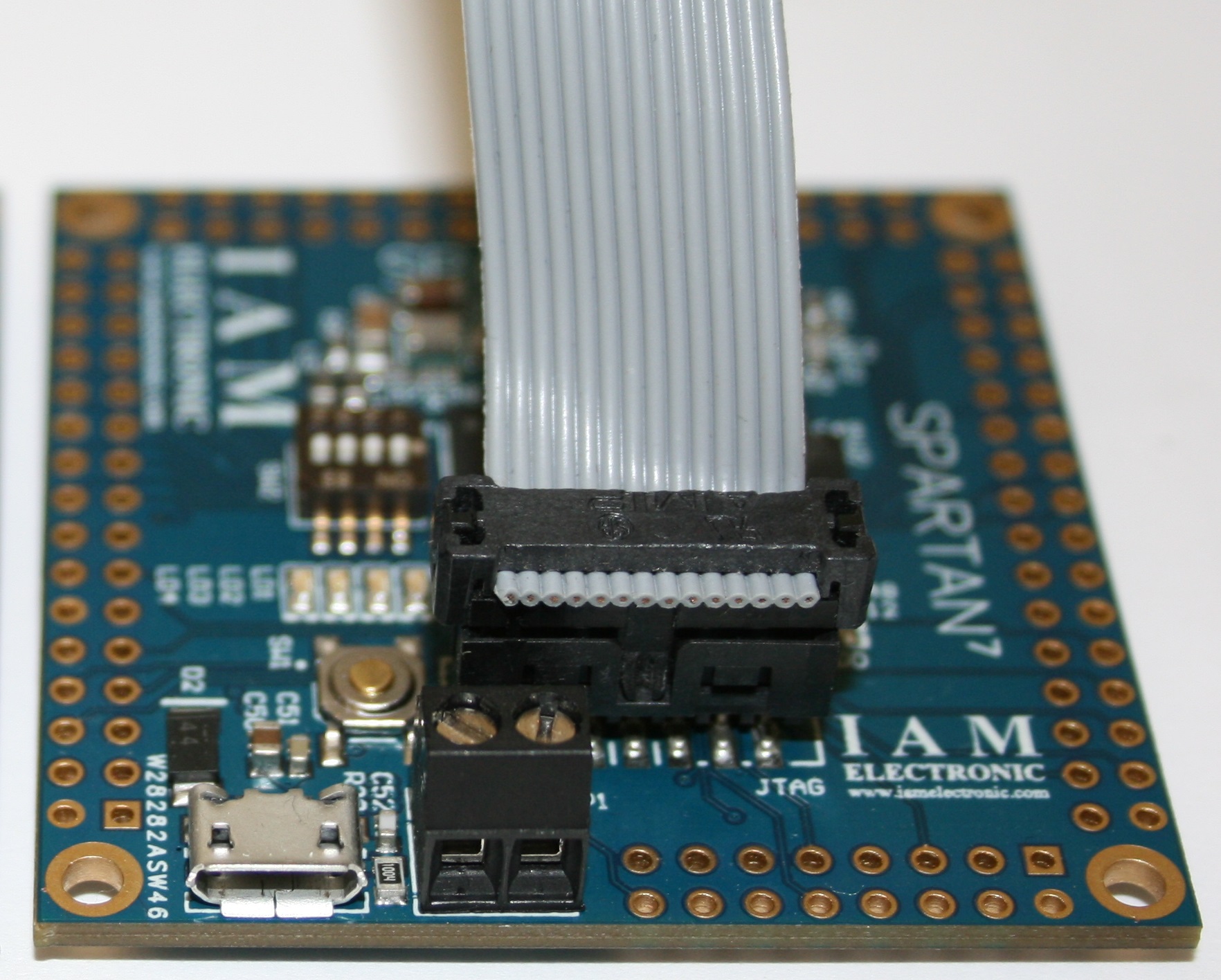 Fig. 3: Onboard standard Xilinx JTAG header (left) with plugged Digilent JTAG-HS3 Programming Cable (middle) or Xilinx Platform Cable USB (right)
The possibilities to program the FPGA are numerous and depend on the preferences of the user. In the simplest case you use the Hardware Manager from Xilinx Vivado and program the FPGA directly with a bit-file.
For a non-volatile configuration of the FPGA you have to program a valid configuration file to the onboard SPI flash. The configuration memory is an IC of S25FL064L series from Cypress Semiconductor. In the Hardware Manager from Xilinx Vivado you have to choose
the type s25fl064l-spi-x1_x2_x4 (see Fig. 4.). Please note that the Flash memory is only supported since Vivado version 2017.3.
Fig. 3: Onboard standard Xilinx JTAG header (left) with plugged Digilent JTAG-HS3 Programming Cable (middle) or Xilinx Platform Cable USB (right)
The possibilities to program the FPGA are numerous and depend on the preferences of the user. In the simplest case you use the Hardware Manager from Xilinx Vivado and program the FPGA directly with a bit-file.
For a non-volatile configuration of the FPGA you have to program a valid configuration file to the onboard SPI flash. The configuration memory is an IC of S25FL064L series from Cypress Semiconductor. In the Hardware Manager from Xilinx Vivado you have to choose
the type s25fl064l-spi-x1_x2_x4 (see Fig. 4.). Please note that the Flash memory is only supported since Vivado version 2017.3.
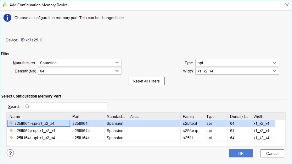 Fig. 4: Choose the right configuration memory part in Xilinx Vivado. The S25FL064L series is supported since Vivado version 2017.3.
You can check proper device functionality by reading XADC values like internal voltage levels or device temperature (see Fig. 5)
Fig. 4: Choose the right configuration memory part in Xilinx Vivado. The S25FL064L series is supported since Vivado version 2017.3.
You can check proper device functionality by reading XADC values like internal voltage levels or device temperature (see Fig. 5)
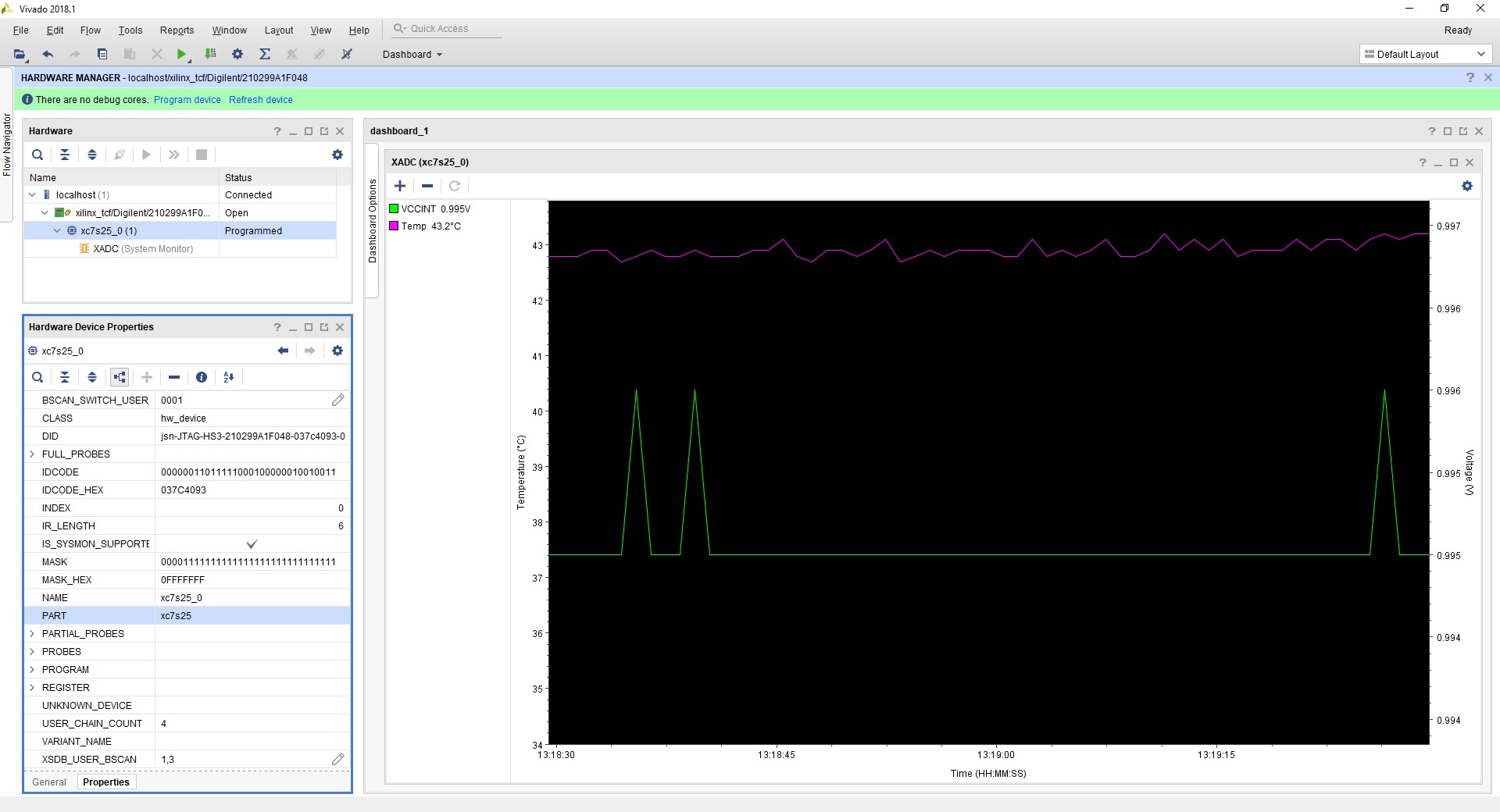 Fig. 5: Xilinx Vivado Hardware Manager can be used to read internal XADC values from the FPGA module.
After you have powered up the board and downloaded the reference design from GitHub (coming soon) to the board, the four user LEDS starts to blink.
Fig. 5: Xilinx Vivado Hardware Manager can be used to read internal XADC values from the FPGA module.
After you have powered up the board and downloaded the reference design from GitHub (coming soon) to the board, the four user LEDS starts to blink.
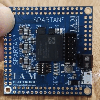 Fig. 6: A "hello world" reference design with blinking LEDs is available at GitHub (coming soon).
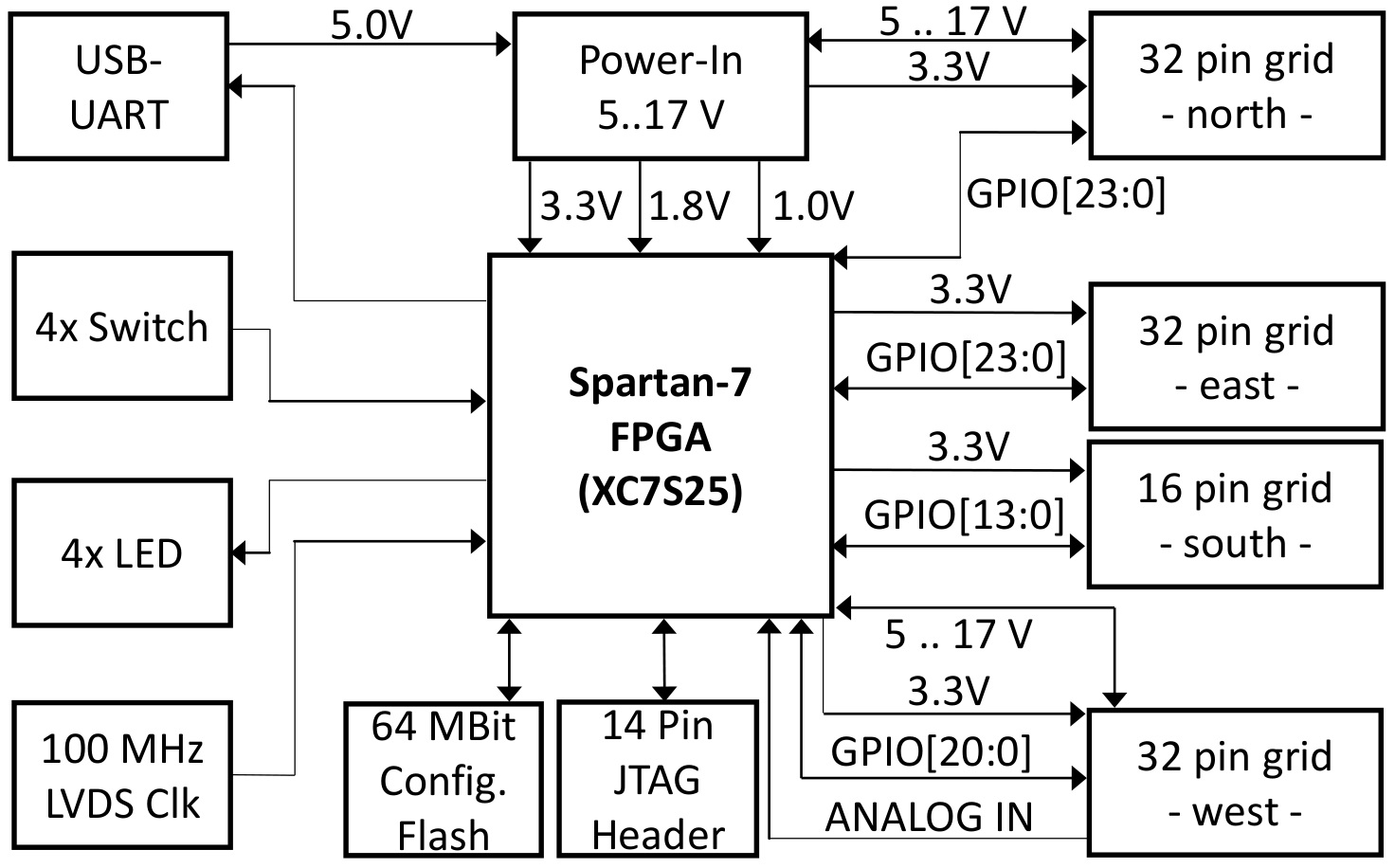
T0006 SPARTAN-7 FPGA BOARD Schematics
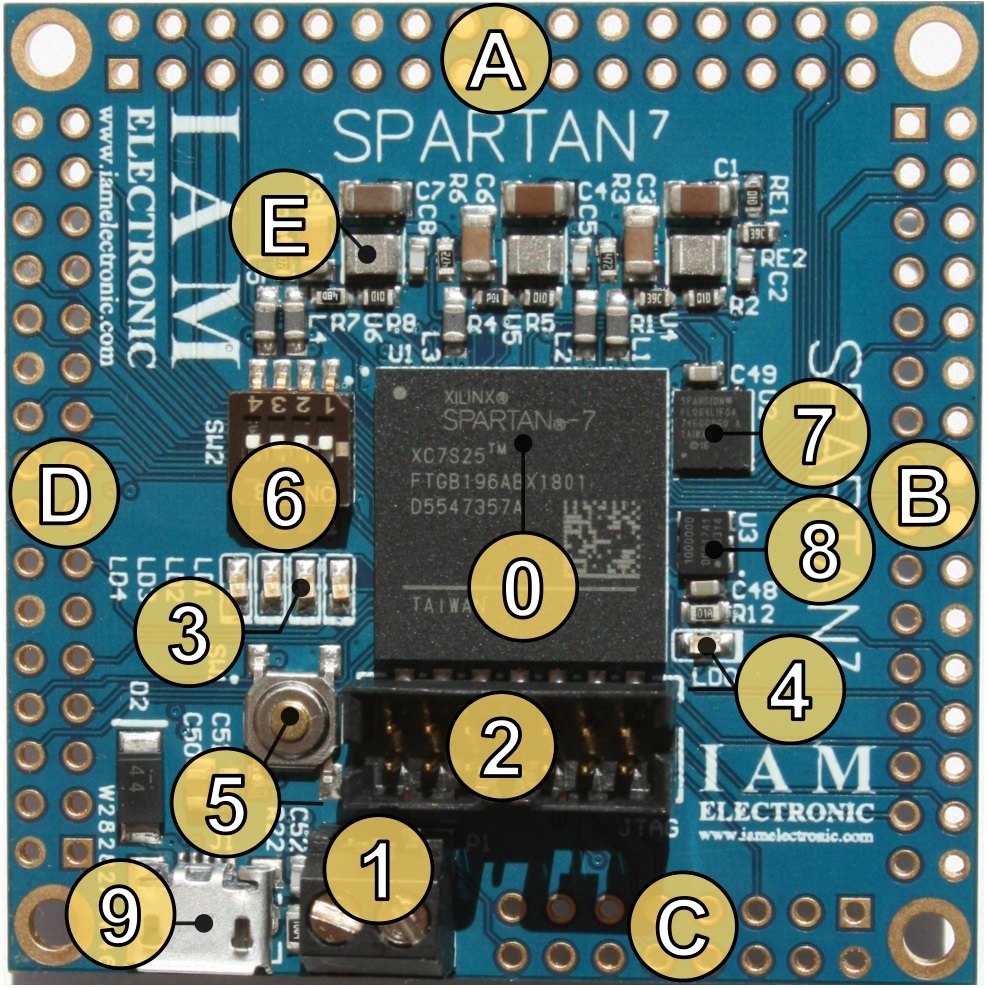 Fig. 7: An overview of all building blocks of Spartan-7 FPGA board.
0. FPGA The board is assembled with a Xilinx Spartan-7 FPGA XC7S25-1FTGB196C. The speed grade of this device is -1 and operating temperture range is 0°C .. 85°C (commercial grade). Other assemblies are available on request (see Ordering information). A master XDC constraint file is available at GitHub (https://github.com/iamelectronic/T0006_Spartan_7_Hello_World) as well as a reference sample project for Xilinx Vivado.
1. P1 screw terminal
The screw terminal P1 is for direct power supply with loose cables. Recommended wire range (AWG) is 16 - 28. The wire strip length should be 3-4mm. The circuitry is designed for an input voltage of 5 V to 17 V.
Make sure the polarity is correct when connecting the cables!
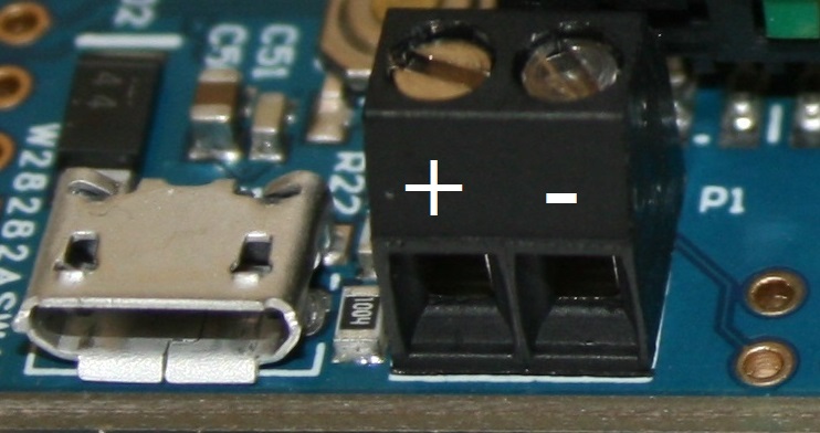 Fig. 8: Screw terminal P1 for power input (front view). Left port is positive terminal, right is negative (GND).
2. JTAG header
The pin assignment of the JTAG header matches the 14 pin pos. connectors of common programming cables. Some examples have been shown in section 2.1. Programming the board.
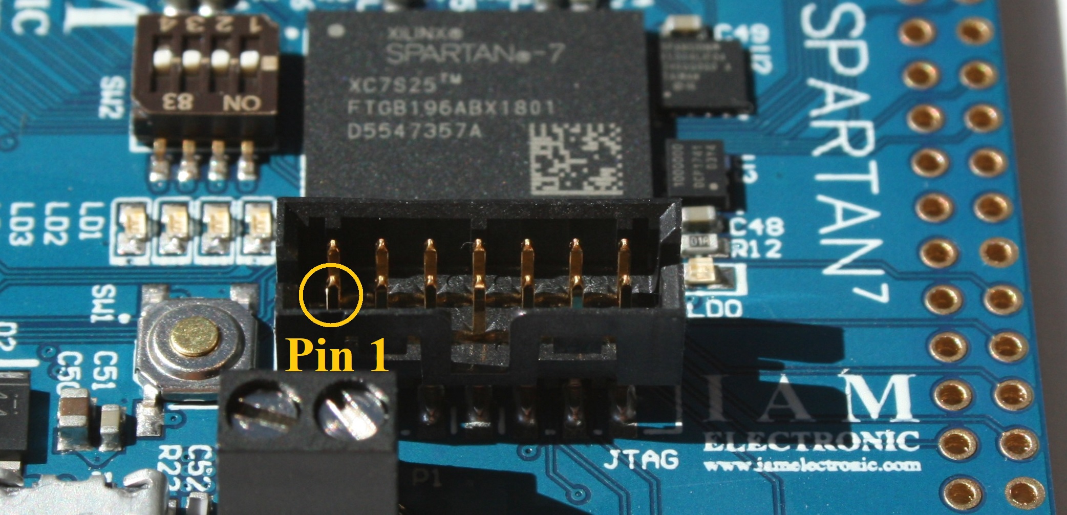 Fig. 9: Standard Xilinx JTAG Header, dual row with 14 pins (2.00 mm pitch).
| Board pin | Note | FPGA pin name | Bank | Location |
| JTAG Pin 1 | GND | |||
| JTAG Pin 2 | 3.3 V | |||
| JTAG Pin 3 | GND | |||
| JTAG Pin 4 | TMS | TMS_0 | 0 | M6 |
| JTAG Pin 5 | GND | |||
| JTAG Pin 6 | TCK | TCK_0 | 0 | A7 |
| JTAG Pin 7 | GND | |||
| JTAG Pin 8 | TDO | TDO_0 | 0 | P6 |
| JTAG Pin 9 | GND | |||
| JTAG Pin 10 | TDI | TDI_0 | 0 | P7 |
| JTAG Pin 11 | GND | |||
| JTAG Pin 12 | N.C | |||
| JTAG Pin 13 | GND | |||
| JTAG Pin 14 | N.C |
3. User LEDs (blue)
Besides the FPGA there is a row of four blue LEDS. They are marked with
designators LD1, LD2, LD3, and LD4. The output drivers of the FPGA pins are used to power the LEDs directly through a 100 Ω series resistor. Tab. 3 shows the output pins from the FPGA connected to the LEDs.
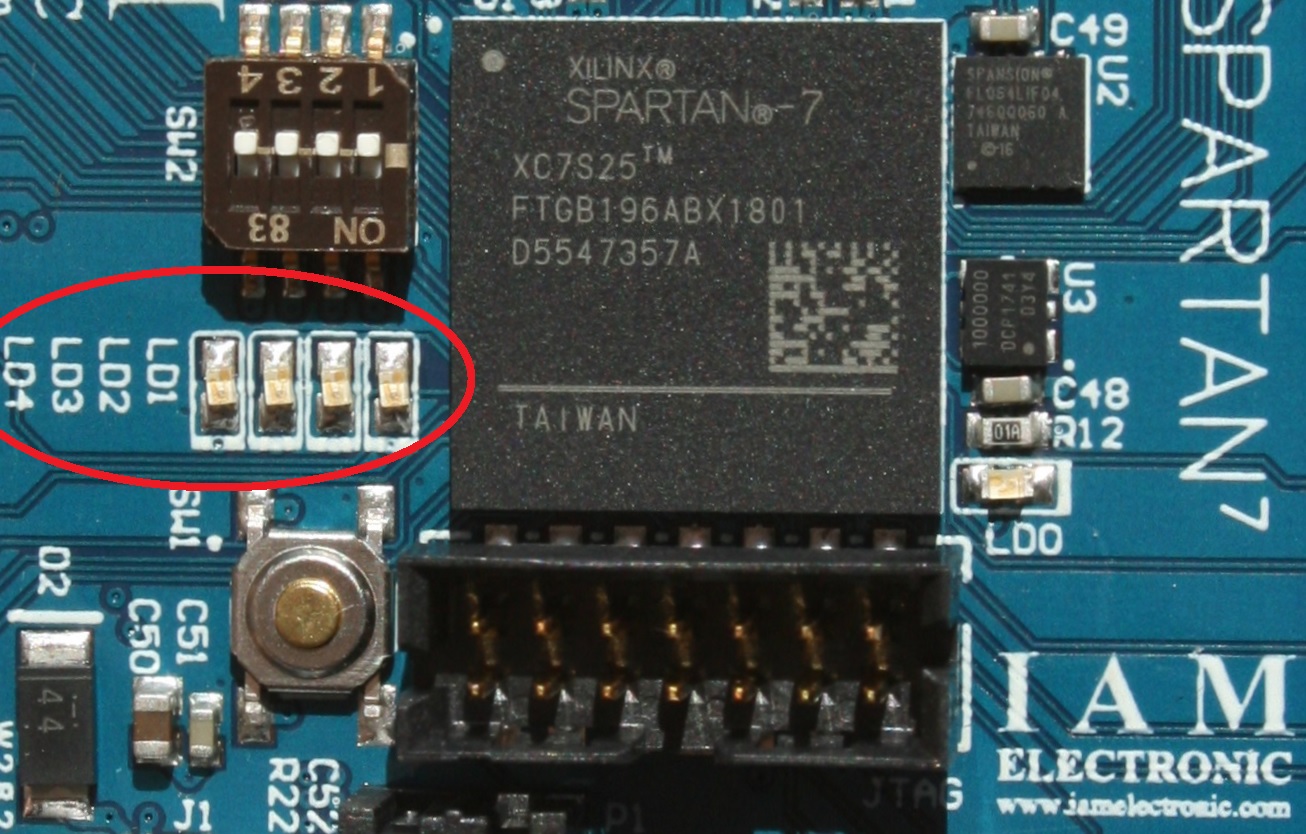 Fig. 10: User LEDs (blue) LD1, LD2, LD3, and LD4.
| Board pin | Note | FPGA pin name | Bank | Location |
| LD1 | High = LED on | IO_L18P_T2_34 | 34 | M1 |
| LD2 | High = LED on | IO_25_14 | 14 | M10 |
| LD3 | High = LED on | IO_0_34 | 34 | B6 |
| LD4 | High = LED on | IO_L18N_T2_34 | 34 | L1 |
4. Configuration LED
LD0 indicates completion of the configuration sequence. After programming has finished, the LED will be on (until the FPGA is configured, the LED will be off). In normal operation the LED LD0 is permanently switch on.
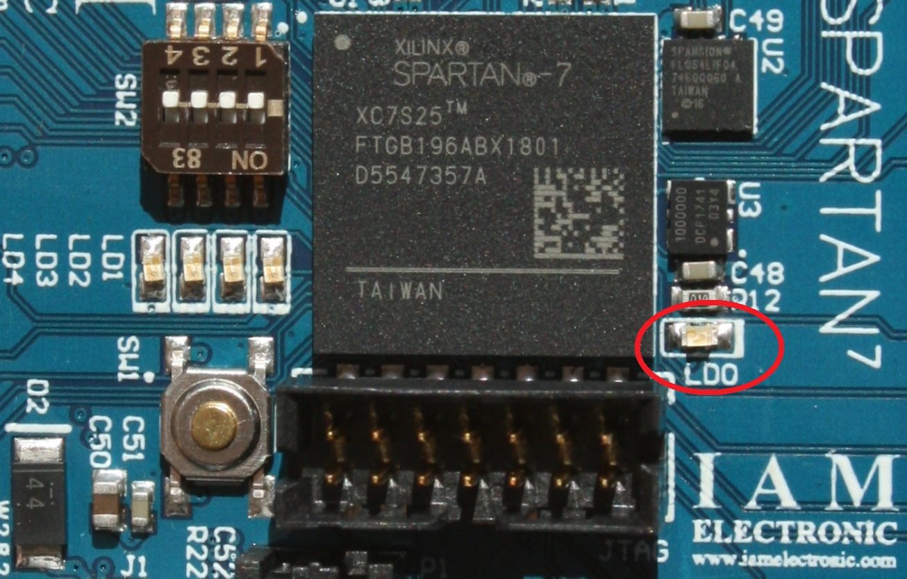 Fig. 11: User LEDs (blue) LD1, LD2, LD3, and LD4.
| Board pin | Note | FPGA pin name | Bank | Location |
| LD0 | Configuration done = LED on | DONE_0 | 0 | P9 |
5. Reset button
The button SW1 next to the JTAG connector triggers a manual reset of the FPGA.
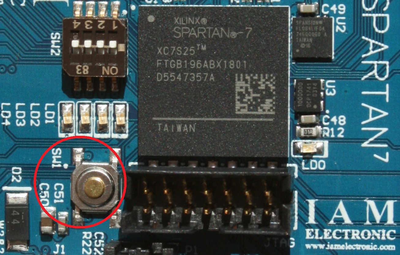 Fig. 12: Reset button SW1.
In the unpressed state the PROGRAM_B pin of the FPGA is pulled high, and while pushing the button this pin is tied to GND. On falling edge, the FPGA configuration is cleared
and configuration sequence is initiated upon the following rising edge. Because the FPGA is permanently configured to Master SPI mode, a new sequence will load configuration data from SPI flash.
Fig. 12: Reset button SW1.
In the unpressed state the PROGRAM_B pin of the FPGA is pulled high, and while pushing the button this pin is tied to GND. On falling edge, the FPGA configuration is cleared
and configuration sequence is initiated upon the following rising edge. Because the FPGA is permanently configured to Master SPI mode, a new sequence will load configuration data from SPI flash.
| Board pin | Note | FPGA pin name | Bank | Location |
| SW1 | Unpressed = High, pressed = Low | PROGRAM_B_0 | 0 | L7 |
6. Micro switches
The four micro DIP switches SW2 can be used for user inputs.
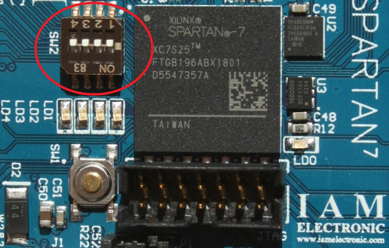 Fig. 13: Micro DIP switches SW2.
Due to the small dimensions of the switches, these can probably be used for coding fixed values or states rather than for user inputs. During OFF-state of the switches, the associated pins
of the FPGA are pulled high. In ON-state, they are tied to GND. The ON position of the switches is marked on the case, and the assigned pins are shown in Tab. 6.
Fig. 13: Micro DIP switches SW2.
Due to the small dimensions of the switches, these can probably be used for coding fixed values or states rather than for user inputs. During OFF-state of the switches, the associated pins
of the FPGA are pulled high. In ON-state, they are tied to GND. The ON position of the switches is marked on the case, and the assigned pins are shown in Tab. 6.
| Board pin | Note | FPGA pin name | Bank | Location |
| SW2 No. 1 | Off = High, On = Low | IO_L17P_T2_34 | 34 | J4 |
| SW2 No. 2 | Off = High, On = Low | IO_L17N_T2_34 | 34 | J3 |
| SW2 No. 3 | Off = High, On = Low | IO_L16P_T2_34 | 34 | K4 |
| SW2 No. 4 | Off = High, On = Low | IO_L16N_T2_34 | 34 | K3 |
7. Configuration memory (SPI flash)
The non-volatile configuration for the FPGA can only be loaded in Master SPI mode (FPGA pins M[2:0]=001) from the attached memory device U2 (SPI flash).
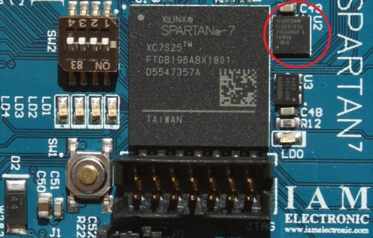 Fig. 14: 64 Mbit SPI configuration flash.
During configuration, internal pull-up resistors are
disabled on each SelectIO pin, because pin B10 IO_L3P_T0_DQS_PUDC_B is permanently pulled high. The flash is from S25FL064L series from Cypress Semiconductor.
Since Xilinx Vivado version 2017.3 these series is supported (see Xilinx UG908, Table C-3: Supported Flash Memory Devices for Spartan-7 Device Configuration).
The flash memory has a density of 64 Mbit. The entire configuration bitstream length for the Xilinx XC7A35T is 17,536,096 bit (see Xilinx UG470, Table 1-1: Bitstream Length).
In Xilinx Vivado, you have to choose s25fl064l-spi-x1_x2_x4 device for configuration memory (see section 2.1. Programming the board for details). The FPGA pins used to control the SPI flash are listed in Tab. 7
Fig. 14: 64 Mbit SPI configuration flash.
During configuration, internal pull-up resistors are
disabled on each SelectIO pin, because pin B10 IO_L3P_T0_DQS_PUDC_B is permanently pulled high. The flash is from S25FL064L series from Cypress Semiconductor.
Since Xilinx Vivado version 2017.3 these series is supported (see Xilinx UG908, Table C-3: Supported Flash Memory Devices for Spartan-7 Device Configuration).
The flash memory has a density of 64 Mbit. The entire configuration bitstream length for the Xilinx XC7A35T is 17,536,096 bit (see Xilinx UG470, Table 1-1: Bitstream Length).
In Xilinx Vivado, you have to choose s25fl064l-spi-x1_x2_x4 device for configuration memory (see section 2.1. Programming the board for details). The FPGA pins used to control the SPI flash are listed in Tab. 7
| Board pin | Note | FPGA pin name | Bank | Location |
| U2 pin 6 | SCK | CCLK_0 | 0 | A8 |
| U2 pin 1 | CS# | IO_L6_T0_FCS_B_14 | 14 | C11 |
| U2 pin 5 | SI/IO0 | IO_L1P_T0_D00_MOSI_14 | 14 | B11 |
| U2 pin 2 | SO/IO1 | IO_L1N_T0_D01_DIN_14 | 14 | B12 |
| U2 pin 3 | WP#/IO2 | IO_L2P_T0_D02_14 | 14 | D10 |
| U2 pin 7 | HOLD#/IO3 | IO_L2N_T0_D03_14 | 14 | C10 |
| Pull-Up R13 | High | M0_0 | 0 | M7 |
| GND | Low | M1_0 | 0 | M8 |
| GND | Low | M2_0 | 0 | M9 |
| Pull-Up R10 | High | IO_L3P_T0_DQS_PUDC_B_14 | 14 | B10 |
8. Clock source 100 MHz
A Low-Jitter precision oscillator generates a stable system clock for the FPGA. The board has a DSC1101CI5-100.0000 MEMS oscillator (U3) from Mirochip with 100 MHz output clock frequency.
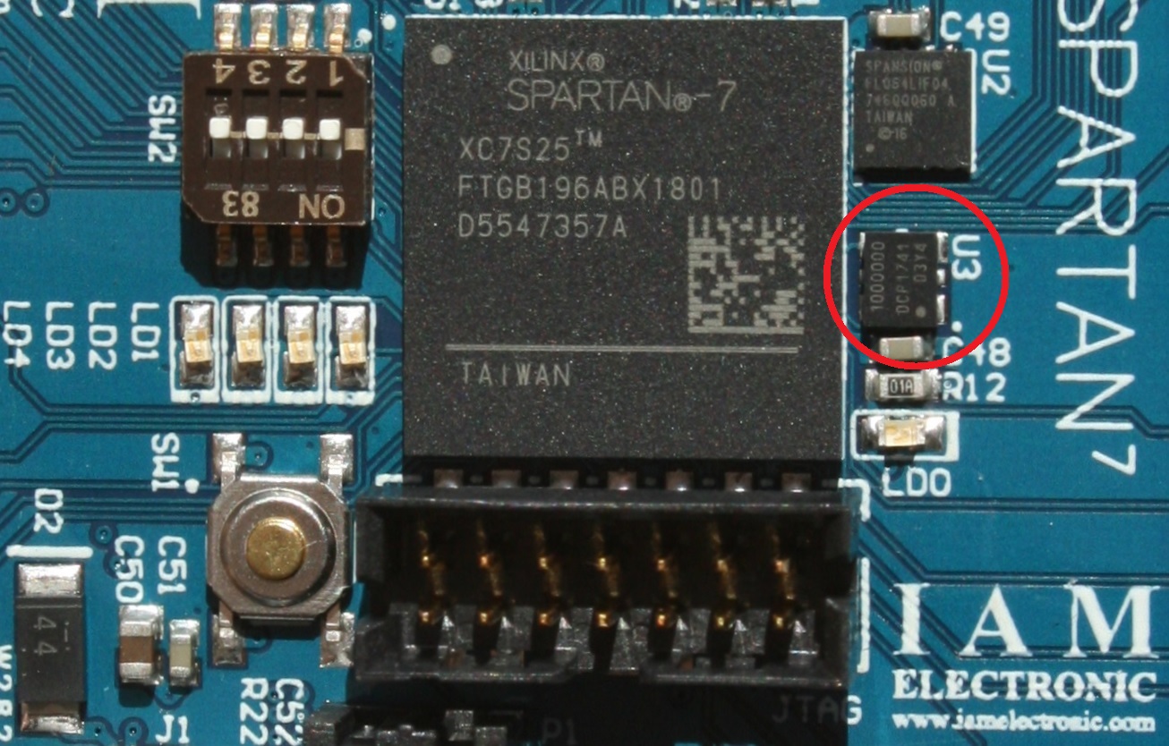 Fig. 15: 100 MHz clock source.
The operating temperature is
from -40°C to 85°C with a frequency stability of ±10 ppm. The clock soure has a signle ended CMOS Output (High = min. 2.97 V, Low = max. 0.33 V). The output is directly routed to a Multi-region Clock Capable (MRCC) clock input on bank 14 (see Tab. 8).
Fig. 15: 100 MHz clock source.
The operating temperature is
from -40°C to 85°C with a frequency stability of ±10 ppm. The clock soure has a signle ended CMOS Output (High = min. 2.97 V, Low = max. 0.33 V). The output is directly routed to a Multi-region Clock Capable (MRCC) clock input on bank 14 (see Tab. 8).
| Board pin | Note | FPGA pin name | Bank | Location |
| U3 pin 4 | 100 MHz Output from U3 | IO_L13N_T2_MRCC_14 (Board REV. A 2018) | 14 | H12 |
| U3 pin 4 | 100 MHz Output from U3 | IO_L13P_T2_MRCC_14 (Board REV. B 2019) | 14 | H11 |
9. USB-UART Bridge
The board includes a CP2102 Single-Chip USB to UART bridge from Silicon Labs. The devices has designator U7 and is located on bottom side of the board. The utilized CP2102N-A01-GQFN20 chip can transmit data with a maximum baud rate of 3 Mbaud.
Please download the CP210x Virtual Com Port (VCP) drivers from silabs.com. After installing the drivers, you can communicate
with your FPGA via a virtual COM port of the operating system.
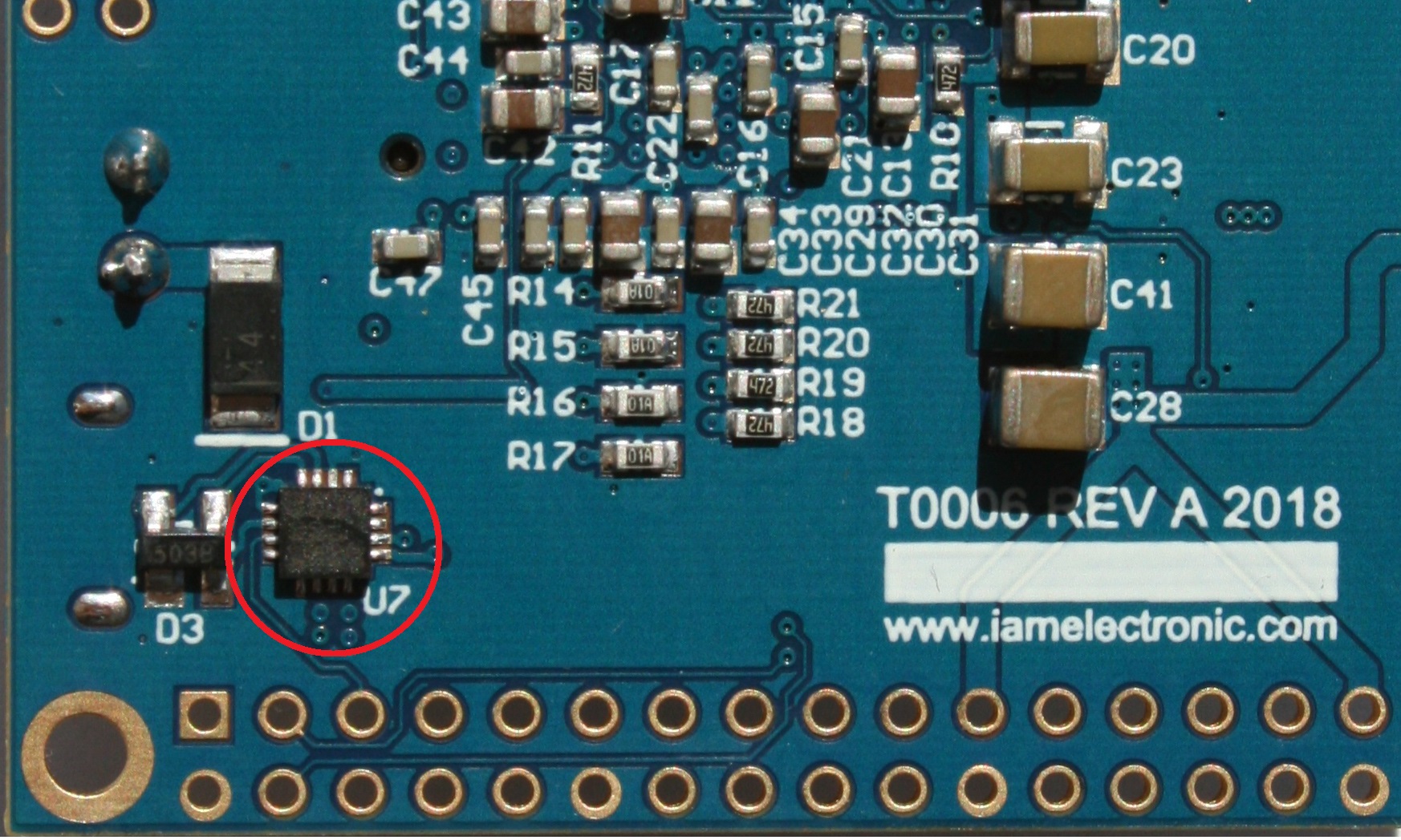 Fig. 16: USB-UART bridge CP2102N-A01-GQFN20 (U7)
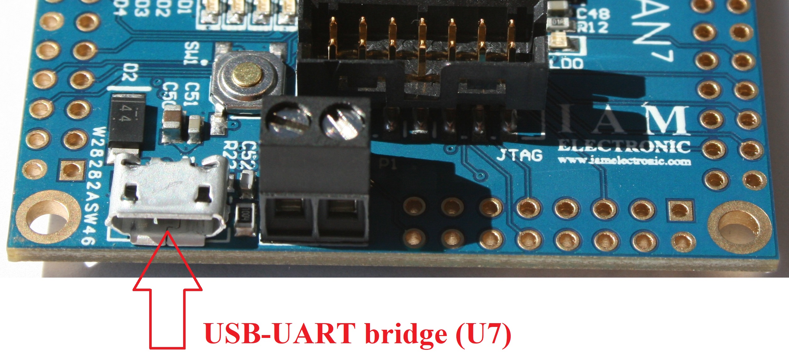 Fig. 17: USB-UART bridge connector J1
| Board pin | Note | FPGA pin name | Bank | Location |
| U7 pin 17 | FPGA TXD -> USB Host RXD | IO_L23N_T3_34 | 34 | M4 |
| U7 pin 18 | FPGA RXD <- USB Host TXD | IO_L23P_T3_34 | 34 | M5 |
A. IO grid PN (NORTH, 32 pins)
The pin grid on the upper side of the board (NORTH) has 32 pins with 2.54 mm pitch. There are 24 General Purpose IOs (GPIOs), three Vout pins with 3.3V, one VIN/VOUT pin (described in 2.1. Powering the board) and four Ground (GND) pins in total.
All IOs are connected to a bank powered at 3.3 V.
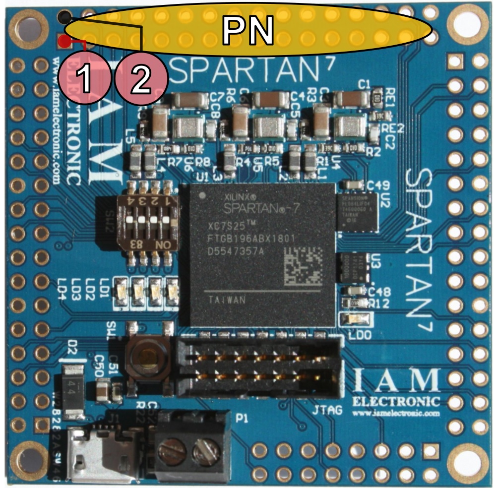 Fig. 16: PN pin grid with 32 positions.
| Board pin | Note | FPGA pin name | Bank | Location |
| PN pin 1 | VIN/VOUT | - | - | - |
| PN pin 2 | GND | - | - | - |
| PN pin 3 | Clock capable (Single Region) | IO_L11P_T1_SRCC_34 | 34 | D1 |
| PN pin 4 | Clock capable (Single Region) | IO_L11N_T1_SRCC_34 | 34 | C1 |
| PN pin 5 | IO_L5N_T0_34 | 34 | B1 | |
| PN pin 6 | IO_L5P_T0_34 | 34 | B2 | |
| PN pin 7 | IO_L1P_T0_34 | 34 | D3 | |
| PN pin 8 | IO_L1N_T0_34 | 34 | C3 | |
| PN pin 9 | IO_L3N_T0_DQS_34 | 34 | A2 | |
| PN pin 10 | IO_L3P_T0_DQS_34 | 34 | B3 | |
| PN pin 11 | 3.3 V | - | - | - |
| PN pin 12 | GND | - | - | - |
| PN pin 13 | IO_L2N_T0_34 | 34 | A3 | |
| PN pin 14 | IO_L2P_T0_34 | 34 | A4 | |
| PN pin 15 | IO_L4P_T0_34 | 34 | B5 | |
| PN pin 16 | IO_L4N_T0_34 | 34 | A5 | |
| PN pin 17 | IO_L6P_T0_34 | 34 | C5 | |
| PN pin 18 | IO_L6N_T0_VREF_34 | 34 | C4 | |
| PN pin 19 | IO_L7P_T1_34 | 34 | E4 | |
| PN pin 20 | IO_L7N_T1_34 | 34 | D4 | |
| PN pin 21 | 3.3 V | - | - | - |
| PN pin 22 | GND | - | - | - |
| PN pin 23 | IO_L3N_T0_DQS_EMCCLK_14 | 14 | A10 | |
| PN pin 24 | IO_L6N_T0_D08_VREF_14 | 14 | C12 | |
| PN pin 25 | IO_L4N_T0_D05_14 | 14 | A13 | |
| PN pin 26 | IO_L4P_T0_D04_14 | 14 | A12 | |
| PN pin 27 | IO_L8P_T1_D11_14 | 14 | D12 | |
| PN pin 28 | IO_L8N_T1_D12_14 | 14 | D13 | |
| PN pin 29 | IO_L5N_T0_D07_14 | 14 | B14 | |
| PN pin 30 | IO_L5P_T0_D06_14 | 14 | B13 | |
| PN pin 31 | 3.3 V | - | - | - |
| PN pin 32 | GND | - | - | - |
B. IO grid PE (EAST, 32 pins)
The pin grid on the right side of the board (EAST) has 32 pins with 2.54 mm pitch. There are 24 General Purpose IOs (GPIOs), three Vout pins with 3.3V, one VIN/VOUT pin (described in 2.1. Powering the board) and four Ground (GND) pins in total.
All IOs are connected to a bank powered at 3.3 V.
 Fig. 16: PE pin grid with 32 positions.
| Board pin | Note | FPGA pin name | Bank | Location |
| PE pin 1 | VIN/VOUT | - | - | - |
| PE pin 2 | GND | - | - | - |
| PE pin 3 | Clock capable (Single Region) | IO_L11N_T1_SRCC_14 | 14 | C14 |
| PE pin 4 | Clock capable (Single Region) | IO_L11P_T1_SRCC_14 | 14 | D14 |
| PE pin 5 | IO_L7P_T1_D09_14 | 14 | F12 | |
| PE pin 6 | IO_L7N_T1_D10_14 | 14 | E12 | |
| PE pin 7 | Clock capable (Multi Region) | IO_L12N_T1_MRCC_14 | 14 | F11 |
| PE pin 8 | Clock capable (Multi Region) | IO_L12P_T1_MRCC_14 | 14 | G11 |
| PE pin 9 | IO_L10P_T1_D14_14 | 14 | F13 | |
| PE pin 10 | IO_L10N_T1_D15_14 | 14 | E13 | |
| PE pin 11 | 3.3 V | - | - | - |
| PE pin 12 | GND | - | - | - |
| PE pin 13 | IO_L9P_T1_DQS_14 | 14 | G14 | |
| PE pin 14 | IO_L9N_T1_DQS_D13_14 | 14 | F14 | |
| PE pin 15 | Clock capable (Single Region) | IO_L14P_T2_SRCC_14 | 14 | H13 |
| PE pin 16 | Clock capable (Single Region) | IO_L14N_T2_SRCC_14 | 14 | H14 |
| PE pin 17 | IO_0_14 | 14 | E11 | |
| PE pin 18 | Clock capable (Multi Region) | IO_L13P_T2_MRCC_14 (Board REV. B 2019) | 14 | H11 |
| PE pin 18 | Clock capable (Multi Region) | IO_L13N_T2_MRCC_14 (Board REV. A 2018) | 14 | H12 |
| PE pin 19 | IO_L17P_T2_D30_14 | 14 | J11 | |
| PE pin 20 | IO_L17N_T2_D29_14 | 14 | J12 | |
| PE pin 21 | 3.3 V | - | - | - |
| PE pin 22 | GND | - | - | - |
| PE pin 23 | IO_L18P_T2_D28_14 | 14 | J13 | |
| PE pin 24 | IO_L18N_T2_D27_14 | 14 | J14 | |
| PE pin 25 | IO_L15P_T2_DQS_RDWR_B_14 | 14 | M13 | |
| PE pin 26 | IO_L15N_T2_DQS_DOUT_CSO_B_14 | 14 | L14 | |
| PE pin 27 | IO_L16P_T2_CSI_B_14 | 14 | L12 | |
| PE pin 28 | IO_L16N_T2_D31_14 | 14 | L13 | |
| PE pin 29 | IO_L21P_T3_DQS_14 | 14 | N14 | |
| PE pin 30 | IO_L21N_T3_DQS_D22_14 | 14 | M14 | |
| PE pin 31 | 3.3 V | - | - | - |
| PE pin 32 | GND | - | - | - |
C. IO grid PS (SOUTH, 16 pins)
The pin grid on the lower side of the board (SOUTH) has 16 pins with 2.54 mm pitch. There are 14 General Purpose IOs (GPIOs), one VIN/VOUT pin (described in 2.1. Powering the board) and one Ground (GND) pins in total.
All IOs are connected to a bank powered at 3.3 V.
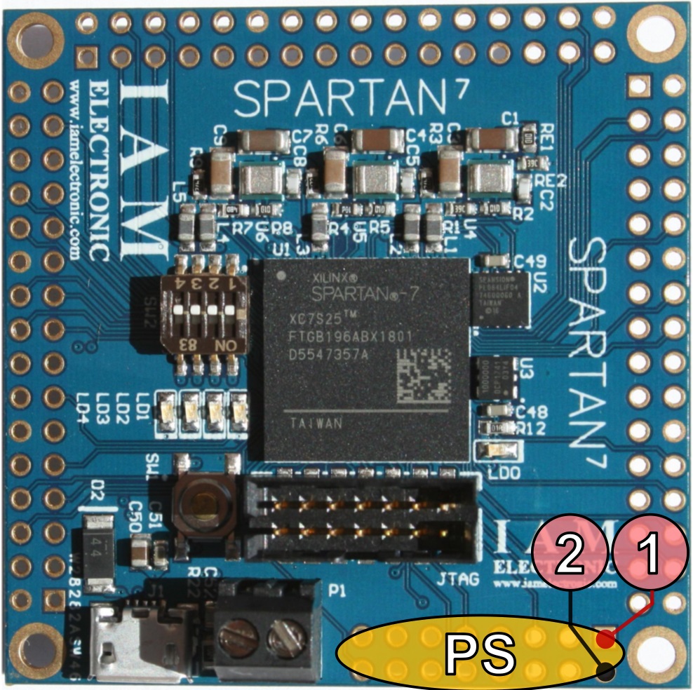 Fig. 16: PS pin grid with 16 positions.
| Board pin | Note | FPGA pin name | Bank | Location |
| PS pin 1 | VIN/VOUT | - | - | - |
| PS pin 2 | GND | - | - | - |
| PS pin 3 | IO_L20N_T3_D23_14 | 14 | M12 | |
| PS pin 4 | IO_L20P_T3_D24_14 | 14 | M11 | |
| PS pin 5 | IO_L5N_T0_34 | 34 | P13 | |
| PS pin 6 | IO_L22P_T3_D21_14 | 14 | P12 | |
| PS pin 7 | IO_L23N_T3_D18_14 | 14 | N11 | |
| PS pin 8 | IO_L23P_T3_D19_14 | 14 | N10 | |
| PS pin 9 | IO_L24N_T3_D16_14 | 14 | P11 | |
| PS pin 10 | IO_L24P_T3_D17_14 | 14 | P10 | |
| PS pin 11 | IO_L19P_T3_D26_14 | 14 | K11 | |
| PS pin 12 | IO_L19N_T3_D25_VREF_14 | 14 | K12 | |
| PS pin 13 | IO_L24P_T3_34 | 34 | P5 | |
| PS pin 14 | IO_L24N_T3_34 | 34 | N4 | |
| PS pin 15 | IO_25_34 | 34 | L5 | |
| PS pin 16 | IO_L21P_T3_DQS_34 | 34 | P4 |
A. IO grid PW (WEST, 32 pins)
The pin grid on the left side of the board (WEST) has 32 pins with 2.54 mm pitch. There are 21 General Purpose IOs (GPIOs), one analog input (differential), three Vout pins with 3.3V, one VIN/VOUT pin (described in 2.1. Powering the board), one state pin, and four Ground (GND) pins in total.
All IOs are connected to a bank powered at 3.3 V.
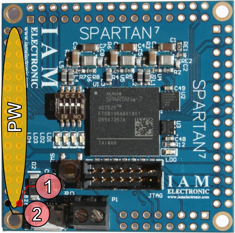 Fig. 16: PW pin grid with 32 positions.
| Board pin | Note | FPGA pin name | Bank | Location |
| PW pin 1 | VIN/VOUT | - | - | - |
| PW pin 2 | GND | - | - | - |
| PW pin 3 | Analog input (positive) | VP_0 | 0 | G8 |
| PW pin 4 | Analog input (negative) | VN_0 | 0 | H7 |
| PW pin 5 | Power good 3.3 V rail | - | - | - |
| PW pin 6 | IO_L21N_T3_DQS_34 | 34 | P3 | |
| PW pin 7 | IO_L20P_T3_34 | 34 | P2 | |
| PW pin 8 | IO_L20N_T3_34 | 34 | N1 | |
| PW pin 9 | IO_L19N_T3_VREF_34 | 34 | M2 | |
| PW pin 10 | IO_L19P_T3_34 | 34 | M3 | |
| PW pin 11 | 3.3 V | - | - | - |
| PW pin 12 | GND | - | - | - |
| PW pin 13 | IO_L22N_T3_34 | 34 | L2 | |
| PW pin 14 | IO_L22P_T3_34 | 34 | L3 | |
| PW pin 15 | IO_L13P_T2_MRCC_34 | 34 | H4 | |
| PW pin 16 | IO_L13N_T2_MRCC_34 | 34 | H3 | |
| PW pin 17 | IO_L15P_T2_DQS_34 | 34 | J2 | |
| PW pin 18 | IO_L15N_T2_DQS_34 | 34 | J1 | |
| PW pin 19 | Clock capable (Single Region) | IO_L14P_T2_SRCC_34 | 34 | H2 |
| PW pin 20 | Clock capable (Single Region) | IO_L14N_T2_SRCC_34 | 34 | H1 |
| PW pin 21 | 3.3 V | - | - | - |
| PW pin 22 | GND | - | - | - |
| PW pin 23 | IO_L9N_T1_DQS_34 | 34 | F1 | |
| PW pin 24 | IO_L9P_T1_DQS_34 | 34 | G1 | |
| PW pin 25 | IO_L8P_T1_34 | 34 | F3 | |
| PW pin 26 | IO_L8N_T1_34 | 34 | F2 | |
| PW pin 27 | Clock capable (Multi Region) | IO_L12P_T1_MRCC_34 | 34 | G4 |
| PW pin 28 | Clock capable (Multi Region) | IO_L12N_T1_MRCC_34 | 34 | F4 |
| PW pin 29 | IO_L10P_T1_34 | 34 | E2 | |
| PW pin 30 | IO_L10N_T1_34 | 34 | D2 | |
| PW pin 31 | 3.3 V | - | - | - |
| PW pin 32 | GND | - | - | - |
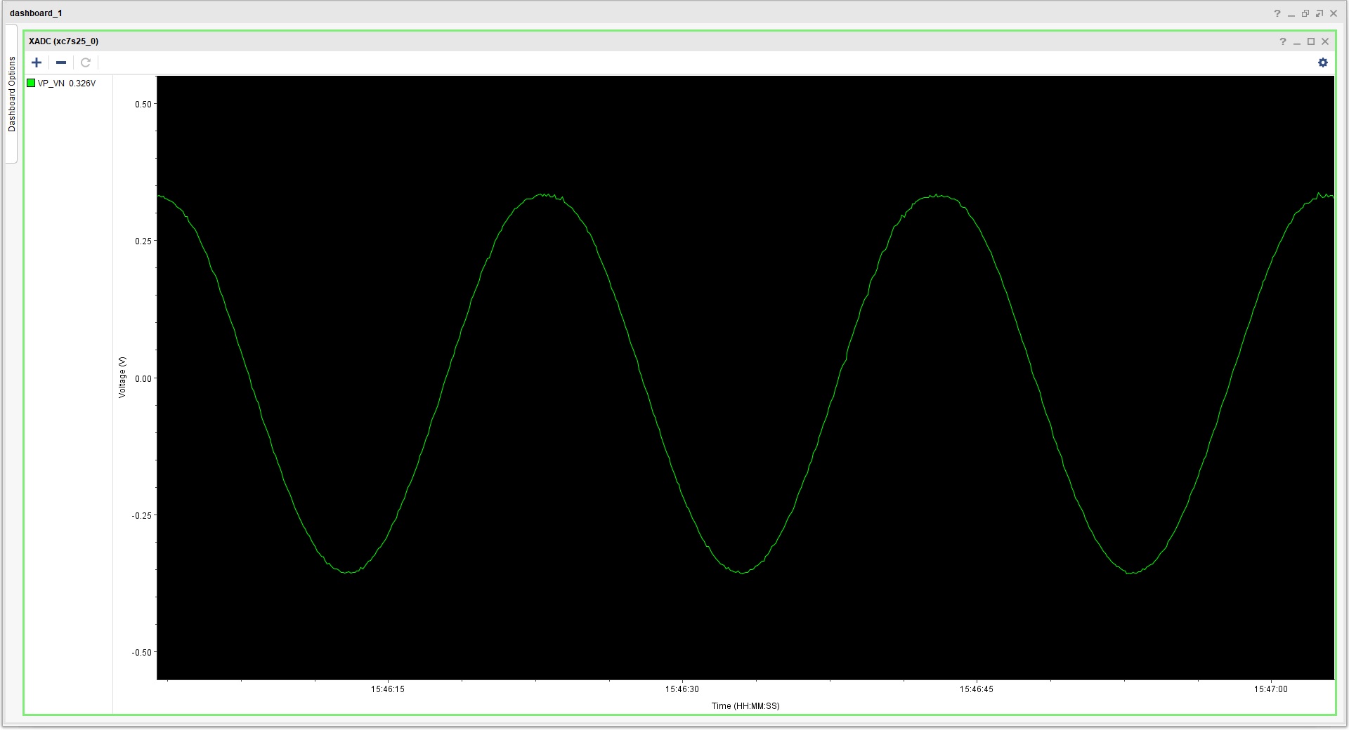 Fig. 15: Example of using the analog input of the FPGA. Xilinx Vivado Hardware Manager can be used to visualize analog input samples.
E. DC/DC converter for I/O voltage All I/O banks (bank 0, 14, and 34) of the FPGA are powered by 3.3 V. The voltage is provided by an onboard DC/DC converter which is capable of driving an output current of 2 A. All current sinks connected to the board and the FPGA itself must be considered to not exceed the current limit of 2 A! Further, we recommend the following constraints regarding the configuration of the FPGA: set_property CFGBVS VCCO [current_design]; set_property CONFIG_VOLTAGE 3.3 [current_design]; For single ended IO we recommend following constraint template for IOSTANDARD of a pin: set_property IOSTANDARD LVCMOS33 [get_ports *]; and for differential IO use Transition Minimized Differential Signaling (TMDS) standard: set_property IOSTANDARD TMDS_33 [get_ports *];
to be done after first mass production run!
Following drawings show relevant mechanical dimensions of the board. All dimensions are in millimeters (mm).
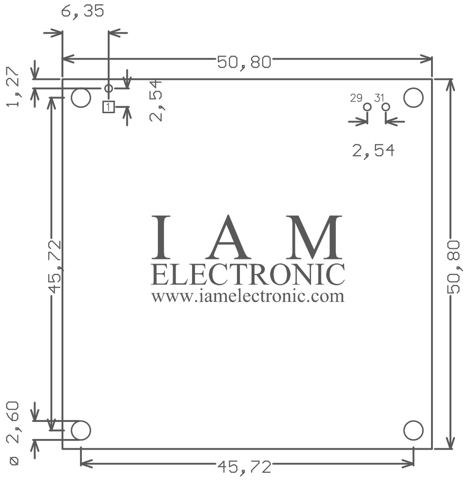 Fig. 18: Mechanical dimension of the FPGA module (board outline and mounting holes).
Tab. 12: Assembly variants of Spartan-7 FPGA Module with product numbers and market places.
| Product no. | Description | Market place | Request quote | Standard lead time |
| T0006 | Spartan-7 FPGA Module with Xilinx FPGAXC7S25-1FTGB196C | IAM Electronic Shop Ebay #184078435546 Tindie #13786 Designspark #505 | info@iamelectronic.com | Normally in stock, otherwise 6 weeks |